
Novel Materials for Perovskite Photovoltaics
Perovskite thin-film photovoltaics promise to reduce dramatically the cost of next-generation photovoltaics. While perovskite photovoltaics demonstrated greatly improved power conversion efficiencies over the past decade, the technology’s future prospects rely on a breakthrough in the development of stable and long-lifetime perovskite materials of high optoelectronic quality. Moreover, lead-free alternatives are desired to facilitate the acceptance of this technology. Given the countless compositions of perovskite semiconductors, a knowledge-based material design approach is needed. For this reason, our team not only examines a large variety of perovskite semiconductors (e.g. “multi-cation”, “inorganic”, “lead-free”, “two-dimensional (2D)”), but is also strongly engaged in the analysis of optoelectronic characteristics such as charge carrier dynamic [1], photon-recycling [2] [3], compositional variation [4] [5], and thin-film morphology [6].
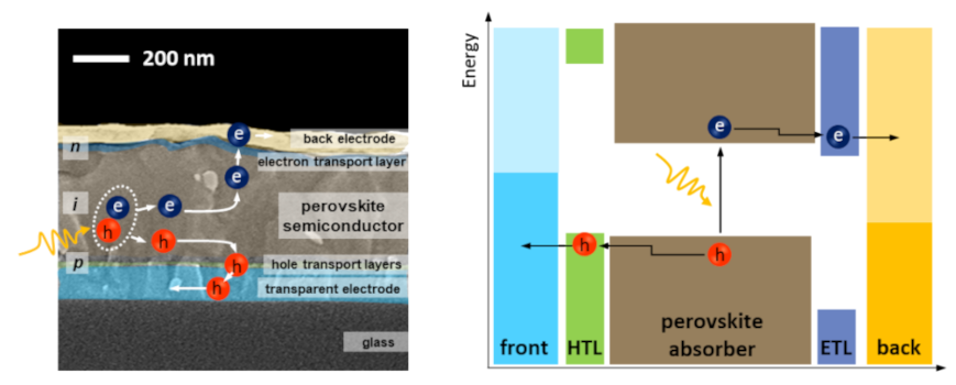
Figure 1: Cross sectional scanning electron image of a thin-film perovskite solar cell and associated energy diagram.
Two-dimensional (2D) perovskite semiconductors and 2D/3D perovskite heterostructures:
Not only three-dimensional (3D) perovskite semiconductors, but also their two-dimensional (2D) analogues exhibit excellent optoelectronic properties. 2D perovskite semiconductors have demonstrated promising stability against environmental factors and act as platform for realizing lead-free alternatives as well as perovskite-based light-emitting diodes and lasers. However, since the 2D structure complicates efficient charge transport, pure 2D perovskite solar cells typically show limited device performance. Employing bulky alkylammonium cations at the surface of a 3D perovskite film forms a so-called 2D/3D heterostructure (see Fig. 1). Our team recently showed that such structures can (i) strongly reduce non-radiative recombination losses in perovskite solar cells [7], [8], [9] and (ii) enhance the excited-state charge transfer in perovskite-based lasers [10]. This leads to astonishingly high open-circuit voltages in solar cells over a wide range of bandgaps (see Fig. 2) and reduces the amplified spontaneous emission (ASE) threshold in lasers as compared to the 3D analogues without the heterostructure.
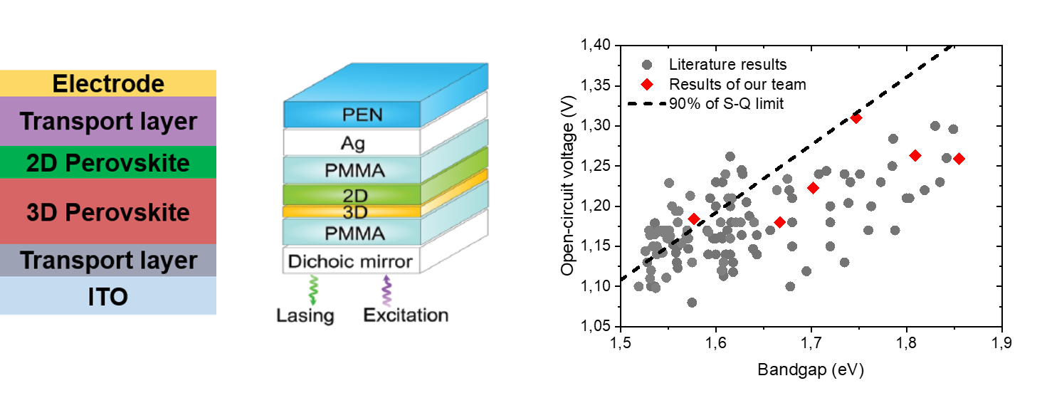
Figure 2: Schematic of a 2D/3D heterostructure in a perovskite solar cell (left) and a perovskite-based laser (middle). Open-circuit voltage of perovskite solar cells for various bandgaps (right). The grey dots represent literatre results, while the red diamond shows results of our team. The dashed line represents 90% of the Shockley-Queisser limit.
Stable and high-quality perovskite semiconductors by compositional engineering:
Compositional engineering of defect-tolerant perovskite semiconductors describes the variation of the organic and inorganic components in the crystal structure. Progress in this field over recent years led to multi-cation perovskite semiconductors that demonstrate improved, but still not sufficient, stability and power conversion efficiency. In order to advance further the stability, we research the underlying mechanisms of light-induced [11] [12], temperature-induced [13] [14], and moisture-induced degradation. We develop guidelines for the material design and device architecture with regard to the composition of multi-cation perovskites [5], passivation layers [15], and charge transport layers [16] [17].
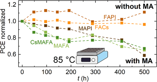
Figure 3: Effect of thermal stress on perovskite thin films with respect to their performance in perovskite solar cells.
Tailored bandgaps of perovskite semiconductors:
Tailored bandgaps are of paramount importance to the realization of high-efficiency perovskite-based tandem photovoltaics. While the optimum bandgap for a perovskite top solar cell is 1.7-1.8 eV in tandem architecture with crystalline silicon (c-Si) or copper indium gallium selenide (CIGS) solar cell, the optimal bandgap of the perovskite bottom solar cell in all-perovskite tandem solar cells is below 1.3 eV. By applying a novel passivation strategy, we demonstrated excellent performance of wide-bandgap perovskite solar cells (~1.7eV). In addition, we research new routes to control the crystallization of low-bandgap perovskite thin films (~1.26 eV) for efficient all-perovskite tandem solar cells [18] [19] [20].
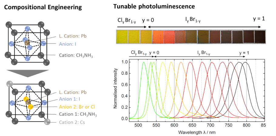
Figure 4: The bandgap of the perovskites can be tuned by compositional engineering.
Textured surfaces:
Processing perovskite solar cells over micrometer-sized pyramidal textures is a timely research topic. We present a comprehensive study about the potential reasons behind the various voltage losses accompanied with processing perovskite thin films over textured surfaces via morphological, microstructural, and compositional analysis. We investigate multiple voltage losses mitigation strategies such as, surface passivation, interfacial engineering, processing parameters, perovskite precursor concentration and stoichiometry, and solvent engineering.
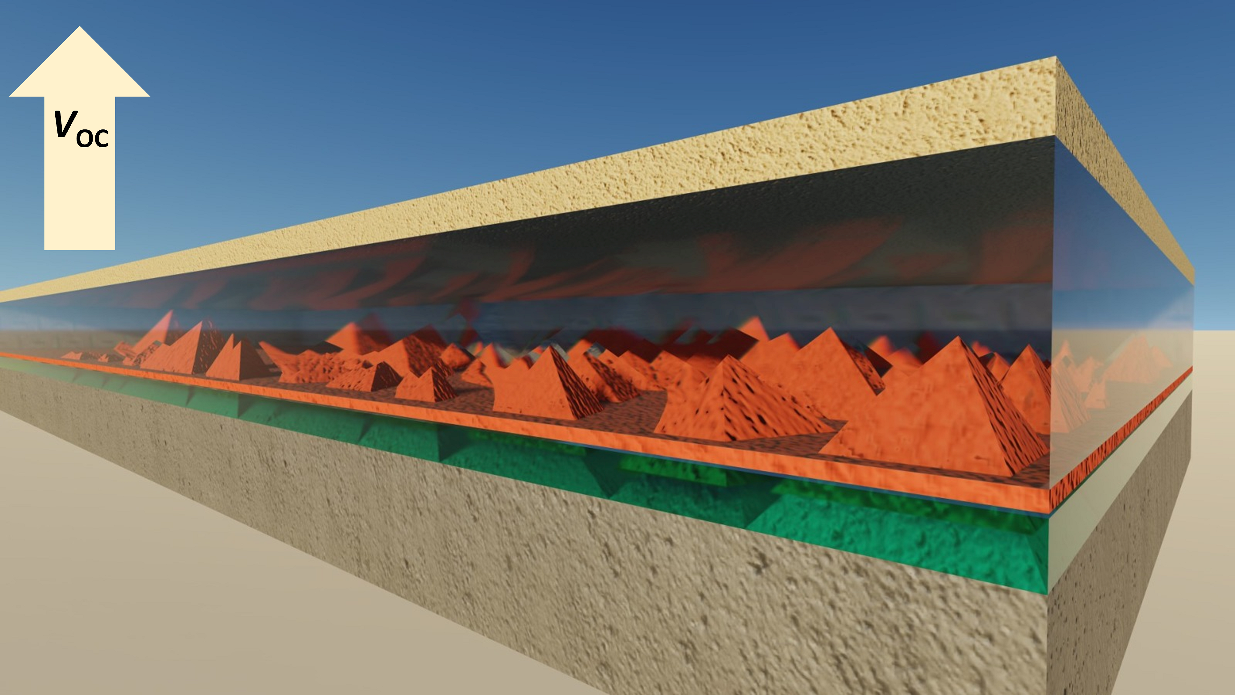
Figure 5: Illustration of a perovskite thin film processed over a textured surface.
Evaporated SAMs:
The importance of self-assembled monolayers as hole transport layers (SAM-HTLs) manifests in the fact that many high efficiency single-junction PSCs and perovskite-based monolithic tandems use the PACz derivatives (i.e. 2PACz, MeO-2PACz, and Me-4PACz). Until now, these materials have been exclusively deposited via solution-based methods, which limits their versatility and restricts process flexibility. To overcome this challenge, we present the first vacuum-based evaporation of common SAM-HTLs.
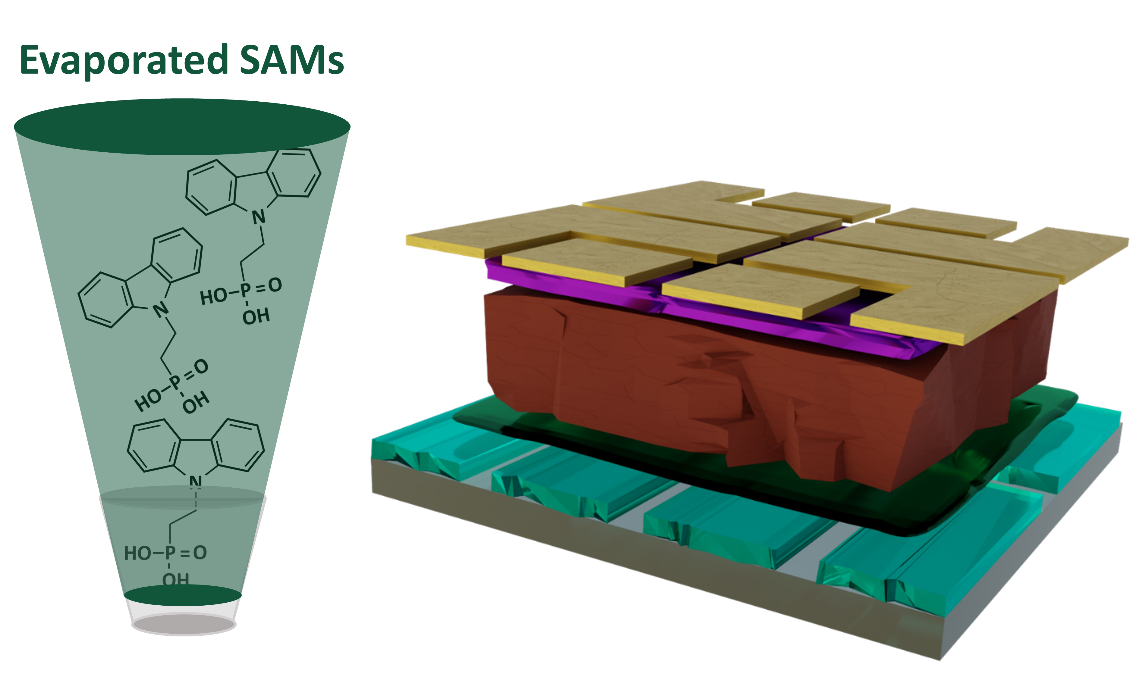
Figure 6: Illustration of vacuum-based evaporation of common SAM-HTLs.