
Perovskite-based Tandem Photovoltaics
The rise of perovskite semiconductors affords a novel opportunity to advance the power conversion efficiency of the market-dominating photovoltaic technologies based on c-Si and CIGS in so-called tandem solar cells. Moreover, perovskite semiconductors of suitable bandgaps can be combined in all-perovskite tandem devices. Advancing these technologies is a focus of our team’s research activities [1] [2]. The key advantage of such a tandem photovoltaics solar module lies in the efficient exploitation of the solar spectrum [3] [4]. The high energy light is harvested at high efficiency in the perovskite top solar cell while the low energy light is harvested in the c-Si, CIGS or perovskite bottom solar cell [5] [6]. With our research partners, we research, develop and prototype highly efficient multijunction perovskite/c-Si solar cells and perovskite/CIGS photovoltaic solar cells.
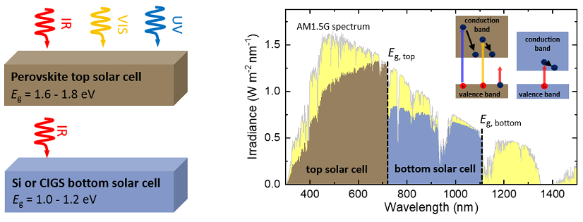
Figure 1: The perovskite-based tandem photovoltaics efficiently uses the AM1.5G solar spectrum. The high energy light is harvested in the top perovskite solar cell, the low energy light is harvested in the bottom solar cell (e.g., c-Si, CIGS or perovskite).
Perovskite-based tandem solar cells with c-Si, CIS or CIGS bottom solar cells.
Our team pursues several avenues to maximize the potential of high-efficiency perovskite-based tandem photovoltaics in association with industrial partners. In the decoupled 4T architecture our extensive work on minimizing optical losses in high quality semitransparent perovskites enabled quality perovskite/CIGs tandem devices with a calculated PCE of 27.3%, with optical simulations outlining further potential improvements [7] [8]. For monolithic 2T tandems, combining computer modelling techniques with material design enabled the creation of record breaking perovskite/CIS monolithic tandems with 23.5% certified PCE [9]. Meanwhile, innovative processing techniques such as lamination have proven a promising technique for decoupling of material constraints, forming high quality and exceptionally stable perovskite/silicon monolithic tandems with power conversion efficiencies (PCEs) of up to 20% [10]. We continue to push our understanding into the requirements and formation of thick perovskites onto textured surfaces through material characterization and computer modelling, which we expect to enable the creation of high quality monolithic tandems on textured silicon in the future [11] [12] [13].
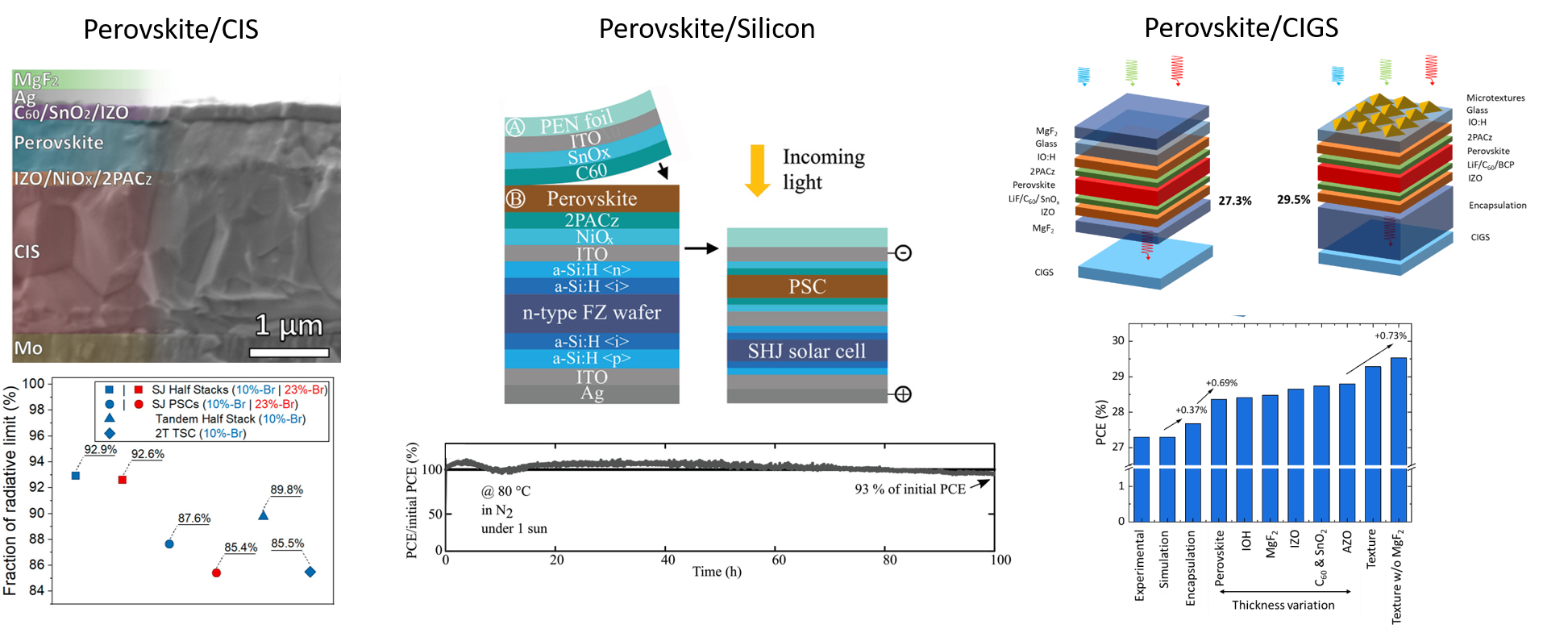
Figure 2: Cross sectional SEM of monolithic perovskite/CIS tandem device along with modelling used to determine optimal perovskite bandgap. Schematic outlining lamination process for formation of monolithic perovskite/silicon tandem devices along with demonstration of excellent stability. Optically optimized device architectures with perovskite/CIGS tandem devices along with breakdown of simulated enhancements.
All-perovskite tandem solar cells.
All-perovskite tandem solar cells combining wide-bandgap (Pb-Based) and narrow-bandgap (Sn-Pb mixed) perovskite semiconductors can overcome the theoretical efficiency of single-junction solar cells. While research on wide-bandgap perovskite solar cells demonstrated advances in stability and performance in recent years, the low bandgap candidates lag behind. In a recent study, we investigated novel solution-processed fullerene derivatives as an interlayer processed in narrow-bandgap perovskite solar cells, achieving 24.8% efficiency in four-terminal all-perovskite tandem solar cells [14]. We modified the two-terminal device architectures for minimizing optical and electrical losses, realizing an high efficiency of up to 23.5% [15].
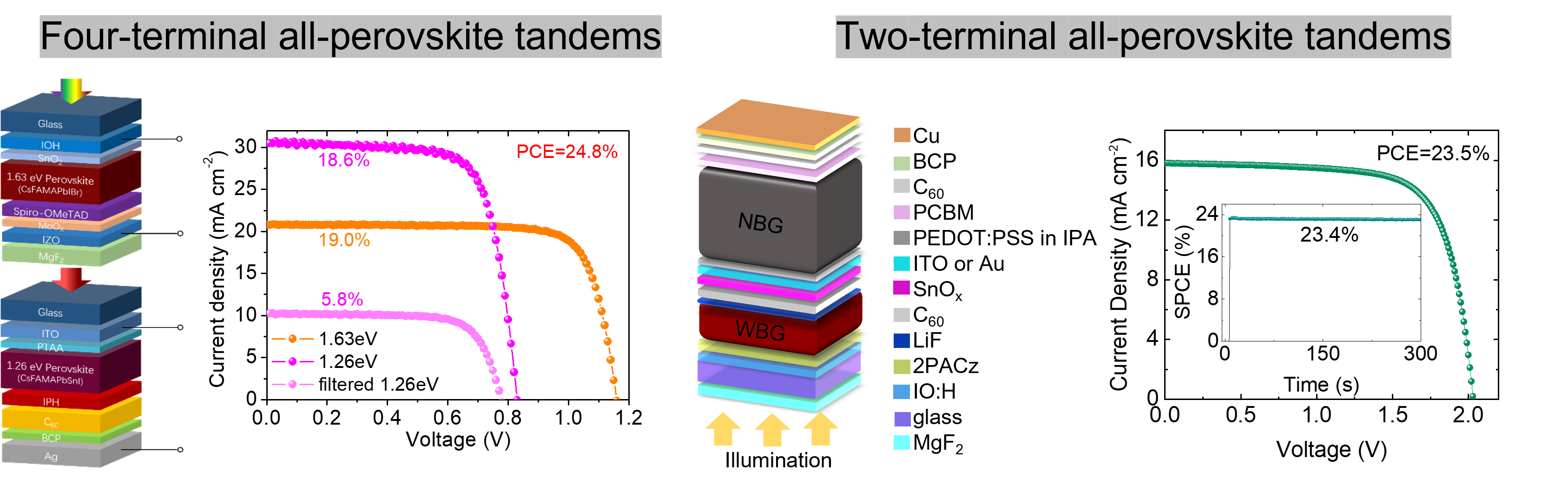
Figure 3: Schematic illustrations and current-voltage characteristics of four-terminal and two-terminal all-perovskite tandems demonstrating 24.8% and 23.5% efficiencies.