
Scalable Processes to Manufacture Perovskite Solar Modules
Perovskite semiconductors combine excellent optoelectronic properties with the ease of solution-processing and co-evaporation as well as low-cost precursor materials. However, the large-scale deposition of pinhole-free and high-quality thin films introduces challenges. In order to advance the scale-up of perovskite solar modules, our team researches these technologies and processes:
Scalable fabrication of solution-processed perovskite thin films
For the solution-based deposition of large-area pinhole-free perovskite thin films, the precursor solutions are printed and must subsequently be dried and crystallized in a controlled way. Our team developed inkjet-printed, blade-coated, slot-die coated perovskite solar cells [1] [2] [3] [4] [5]. Highlights of our research include demonstrations of record efficiencies for perovskite solar cells with inkjet-printed absorbers, as well as perovskite solar cells with a variety of inkjet-printed layers [1]. Another focus of our work is based on the characterisation of the perovskite layer from deposition on the substrate to crystallised perovskite. For this purpose, our group has developed an imaging multichannel photoluminescence device that analyses the growing perovskite layer during drying, nucleation and crystallisation. This allows, for example, a breakdown of perovskite formation by vacuum-assisted growth, which is considered one of the most promising control mechanisms in perovskite formation [6].
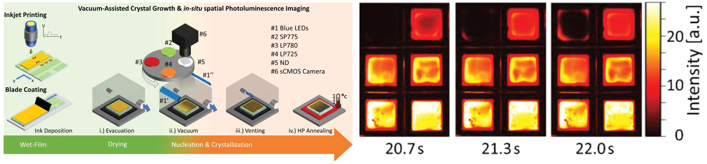
Figure 1: left: Schematic illustration of the inkjet printing process and blade coating, as well as the vacuum-assisted growth process under observation of the developed in-situ photoluminescence process. right: Photoluminescence images of perovskite layers printed with different resolutions after different times [6].
Process control and in situ characterization of solution-processed perovskite thin films
Controlling the nucleation and crystal growth of pinhole-free perovskite thin films over large areas is not only an engineering challenge, but requires understanding the drying dynamics and entangled processes during the formation of the multi-crystalline thin films [6]. For this reason, we are particularly interested in applying in situ optical spectroscopy to analyse the drying, nucleation and crystallization processes. A highlight of our team in this field is our study on in situ characterization of the drying dynamics of blade coated perovskite solar cells [7]. The study reports on a model for the drying dynamics, leading to improved solar cell performance. In order to expand these research activities, we have established a dedicated in situ characterization platform of solution-processed perovskite thin films. This unique platform combines interferometry, (transient) photoluminescence, white light interferometry, and Raman spectroscopy.
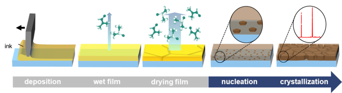
Figure 2: The individual steps of solution-based deposition of perovskite thin films. Optimizing the nucleation and crystallization is important for high-quality perovskite absorbers.
Evaporated perovskite thin-film photovoltaics
Vacuum-based deposition techniques are a common route for the fabrication of large-area thin-film photovoltaics, providing excellent homogeneity and high fabrication yield. In the field of perovskite photovoltaics, however, co-evaporated vacuum-based deposition of perovskite thin films is less researched and limited so far to a few material compositions. Consequently, the demonstrated power conversion efficiencies lag behind solution-processed devices. Our team develops all-evaporated perovskite photovoltaics as a promising approach toward industrial large-scale fabrication [8] [9]. Our labs are equipped with dedicated evaporation systems that enable co-evaporation of complex compositions of perovskite semiconductors (e.g. multi-cation and wide-bandgap candidates) and deposition on areas up to 6 inches.
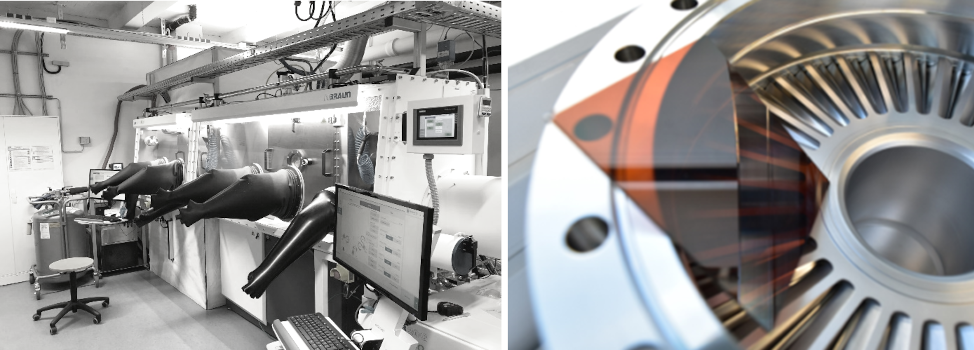
Figure 3: Gloveboxes of our upscaling laboratory and photograph of an evaporated perovskite thin-film.
Perovskite thin-film solar modules
Besides the production of progressively larger high-quality perovskite layers, upscaling includes the fabrication of the interconnection lines (see Figure 4a), which create the solar module (see Figure 4b) by connecting multiple cell stripes in series. Laser ablation, also called laser-scribing, is a promising approach for the fabrication of the interconnection lines, as lasers potentially allow a high-precision, fast, cost-efficient and flexible fabrication of the necessary structures. In laser scribing, focused laser pulses hit the respective layers of the solar cell and, due to evaporation or stress-induced detachment of the material, create necessary trenches. The trenches then enable the series connection of cell stripes integrated in the manufacturing process of the layers. To optimize the technique, the ablation behavior, the redeposition of ablation debris and laser-induced alteration of material are investigated. Highlights of our work include highly selective laser-scribing for fabrication of interconnections lines with minimal detrimental effect on electrical properties of modules (see Figure 4c). By combining this with homogeneous all-evaporated layers as well as a precise laser-scribing alignment, the resulting relative efficiency loss from cells to modules can be reduced to below 7%rel and total interconnection widths of down to 150µm [10].
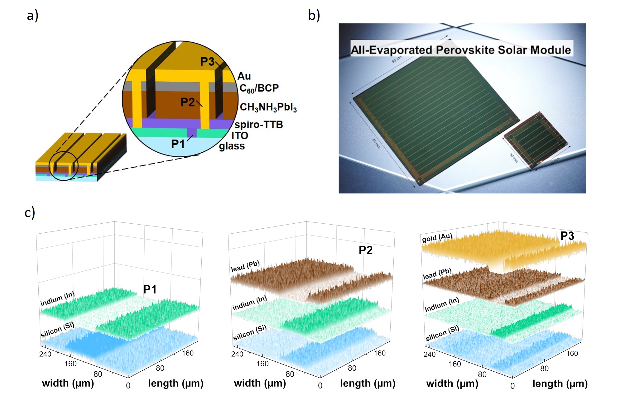
Figure 4: Perovskite solar module interconnection. a) Schematic of the serial interconnection of thin-film solar cells to modules using P1, P2 and P3 lines with an exemplary layer stack of perovskite-based solar cells. b) Picture of two all-evaporated perovskite module with monolithic interconnections on 80 x 80 mm2 and 30 x 30 mm2 substrates. c) Energy dispersive X-ray diffraction measurements demonstrating the high selectivity, residual-free ablation and small dimensions of the laser-scribed interconnection lines [10].
Slot-die coated perovskite thin-film photovoltaics
The transfer of today’s lab-scale processes to large areas via slot-die coating (SDC) still faces substantial challenges. The reason is that established, industrial deposition techniques such as SDC are difficult to control during the entirety of the complex perovskite film formation. Therefore, it is an incredibly interesting subject of research to investigate & enhance the understanding of the impact of coating & drying related transport mechanisms, phenomena & parameters. Systematic strategies for process transfer require an enhanced understanding of the involved fluidics & dynamic processes. Recapitulatory, this kind of scientific experimental work teaches an unique insight in the theoretical complexity of perovskite formation as well as the limits & understanding of the necessary reality check.
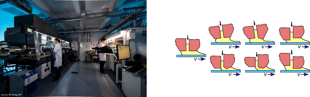
Figure 5: Gloveboxes in our upscaling laboratory containing the slot-die coater and Schematic of solution dispensation during slot-die coating with different metal slit (lip) configurations, changing the thickness and quality of the deposited wet film.
(In situ) Photoluminescence Imaging
When scaling perovskite solar cell fabrication to large areas, process monitoring of the film formation is vital for achieving lateral control of perovskite thin-films quality. Photoluminescence (PL) imaging excells at this task on any scale – capable of non-invasively characterizing perovskite absorber films or complete perovskite solar cells in a matter of milliseconds. For instance, PL imaging can be used to assess the homogeneity of already fabricated perovskite thin-films [11] [12] or for in situ monitoring of the formation of the perovskite material [13] [14] [15], yielding decicive information of its optelectronic quality early-on.
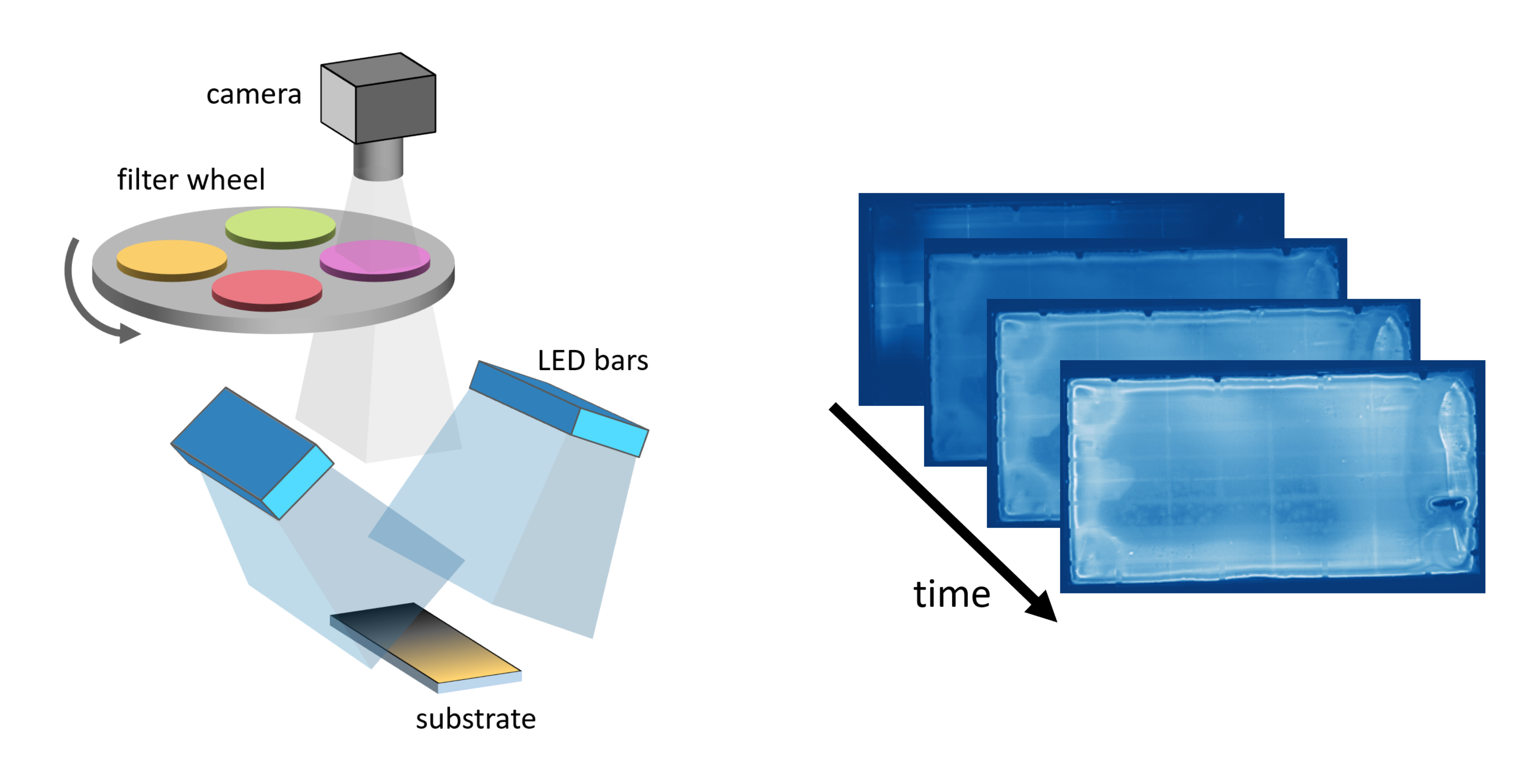
Figure 6: Schematic illustration of the photoluminescence (PL) imaging setup (left). Examplary time series of PL images of a blade-coated perovskite thin-film (right).
Scalable monolithic all-perovskite tandem solar modules
Among fast-growing perovskite-based tandem solar cells, two terminal all-perovskite tandem solar cells attracted substantial attention regarding their low cost of fabrication, mechanical flexibility, fully solution-based processability, and flexibility in designing different architectures with different perovskite bandgaps. Therefore, they are assumed to hold a considerable share in the future PV market, provided that the challenges of stability and scalability are met.
The PV research team led by led by Dr. Bahram Abdollahi Nejand and Tenure-Track-Professor Ulrich W. Paetzold, was able to successfully develop a sound prototype for upscaling high-efficiency two terminal all-perovskite tandem solar cells (with efficiencies of up to 23.5% for an active area of 0.1 cm²) into all-perovskite tandem solar mini-modules with an efficiency of 19.1% for an aperture area of 12.25 cm² and GFF of 94.7-96.3%, while preventing high-efficiency loss (only ~2% relative) through the upscaling procedure (Figure 7). This enormous achievement, which is reported for the first time worldwide, paves the way for further development of upscaling large-area all-perovskite tandem solar modules.
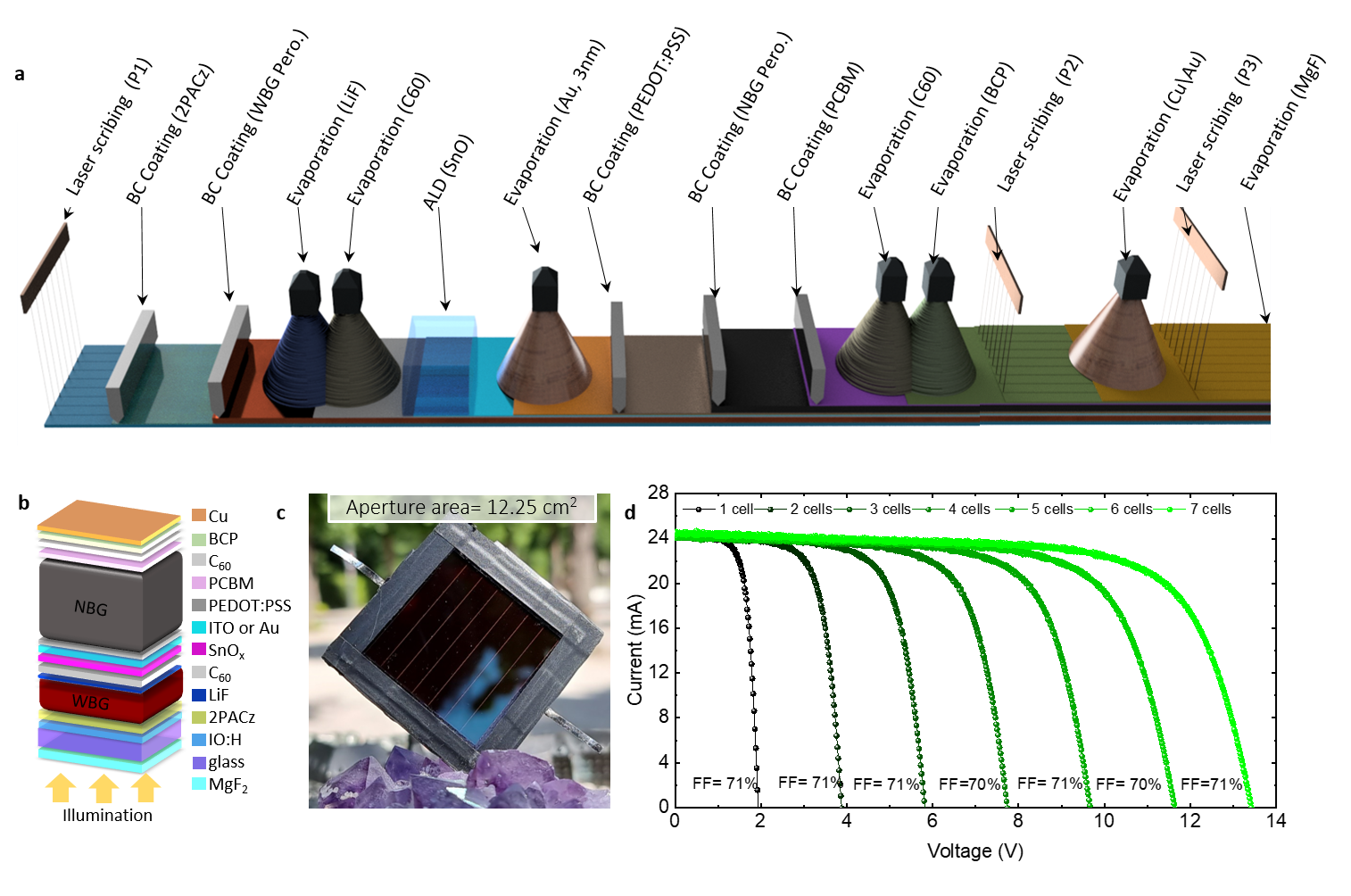
Figure 7: a) Fabrication processing for scalable all-perovskite tandem solar modules (combination of blade-coating and vacuum-deposition techniques). b) Monolithic architecture of all-perovskite tandem. c) The photograph from the front side of the tandem module. with an aperture area of 12.25 cm2. d) Current density–voltage (J–V) characteristic of stepwise accumulated tandem cell stripes of the module. Adapted from publication by B. Abdollahi Nejand et. al [11].