Organic Light Emitting Diodes
Organic light emitting diodes (OLEDs) are an industrially available cutting-edge technology. Advantageous optoelectronic properties, such as high contrast ratio, diffuse light emission or excellent color rendering indices, render them ideal for display applications or general lighting. For OLED industrial fabrication, so far, most organic semiconductors have been applied by thermal evaporation. An alternative and widely discussed deposition method for a more cost-efficient layer deposition is solution processing of organic semiconductors employing printing or coating techniques.
 |
The challenge of solution processing Whereas conventional deposition by thermal evaporation enables high device performance and stability by stacking an arbitrary number of functional layers, the fabrication of such multi-layer devices from solution remains very challenging. To enhance charge carrier injection into solution processed OLEDs, we examined charge carrier injection layers from various metal oxides that were deposited either via precursor routes or from nanoparticles. For hole-injection we applied thin layers of molybdenum-, vanadium- or tungsten oxide from different precursors. Common metal oxide precursors are converted at high temperatures (>300°C) and hence cannot be applied on flexible substrates like polyethylene terephthalate (PET), which withstands temperatures of up to 120°C only. Tungsten(VI)ethoxide precursors, however, can be converted at room temperature under ambient or nitrogen atmosphere. For electron injection we employed solution processed zinc oxide and modified the interface using the polymer polyethylenimine. |
 |
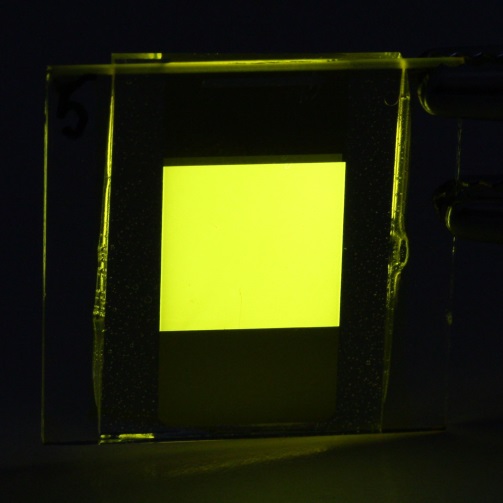
Tandem OLEDs To generate white light, two complementary emitting OLEDs, e.g., a blue and an orange OLED, can be incorporated into a single device. For the serial connection of the OLEDs in such a tandem configuration, an intermediate contact, the so called charge generation layer (CGL), is required. This intermediate contact usually comprises a hole and an electron injection layer in order to simultaneously inject electrons or holes in the adjacent OLEDs. Here, we combined two metal oxide injection layers with a poly(3,4-ethylenedioxythiophene):poly(styrene sulfonate) (PEDOT:PSS) solvent barrier in between. The integrity of the layer stack was verified by secondary ion mass spectrometry and transmission electron microscopy in combination with energy-dispersive X-ray spectroscopy. The tandem OLED exhibits a current efficiency of twice the efficiency of the single-junction devices. To achieve white light emission, we used an orange in the upper and a blue emitting semiconductor in the lower OLED. |
|
|
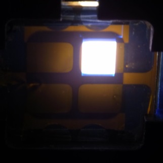
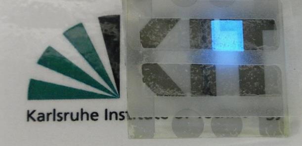
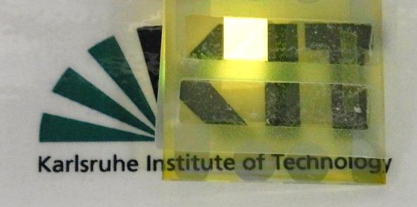
Printable electrodes and mechanical device flexibility The high costs for indium, high process temperatures and its brittleness render the commonly used transparent indium tin oxide (ITO) electrodes unsuitable for future roll-to-roll production. We fabricated ITO-free, all solution processed, transparent OLEDs with inverted architecture by incorporating the conductive polymer poly(3,4‑ethylenedioxy-thiophene):poly(styrene sulfonate) (PEDOT:PSS) to form both electrodes. The opaque metals used in state-of-the-art architectures are replaced by silver nanowire meshs. The electrodes exhibit a transmittance of more than 80% in the visible spectral regime. Upon the incorporation of either a yellow or a blue emitting polymer, we yield performances of our transparent devices comparable to opaque OLEDs with ITO and aluminum electrodes. With respect to the feasibility of the fabrication process and its applicability to future roll-to-roll printing, this device architecture opens new avenues for all-printed transparent organic light emitting diodes. |
Further reading:
- M. Zhang et al., All-solution processed transparent organic light emitting diodes, Nanoscale, 2015, 7, 20009 - 20014, DOI: 10.1039/C5NR05820A.
- S. Höfle et al., Charge Generation Layers for Solution Processed Tandem Organic Light Emitting Diodes with Regular Device Architecture, ACS Appl. Mater. Interfaces, 2015, 7, 8132−8137, DOI: 10.1021/acsami.5b00883.
- S. Höfle et al., Enhanced Electron Injection into Inverted Polymer Light-Emitting Diodes by Combined Solution-Processed Zinc Oxide/Polyethylenimine Interlayers, Adv. Mater., 2014, 26, 2750-2754, DOI: 10.1002/adma.201304666.
- S. Höfle et al., Solution Processed, White Emitting Tandem Organic Light-Emitting Diodes with Inverted Device Architecture, Adv. Mater., 2014, 26, 5155-5159, DOI: 10.1002/adma.201400332.
- S. Höfle et al., Molybdenum oxide anode buffer layers for solution processed, blue phosphorescent small molecule organic light emitting diodes, Organic Electronics, 2013, 14, 1820-1824, DOI: 10.1016/j.orgel.2013.04.017.
- S. Höfle et al., Tungsten Oxide Buffer Layers Fabricated in an Inert Sol-Gel Process at Room-Temperature for Blue Organic Light-Emitting Diodes, Adv. Mater., 2013, 25, 4113-4116, DOI: 10.1002/adma.201301627.